
The world’s first 3nm chip is officially released: not Apple’s
[ad_1]
Although TSMC’s 3nm chips have been mass-produced, as of yesterday, we have not seen chip companies release related products. Today, this situation has finally been broken.
American chip company Marvell said that the company’s data center chip based on TSMC’s 3-nanometer (3nm) process was officially released.
According to Marvell, the company’s industry-first silicon building blocks in this node include 112G XSR SerDes (serializer/deserializer), Long Reach SerDes, PCIe Gen 6 / CXL 3.0 SerDes and 240 Tbps parallel chip-to-chip interconnect .
According to Marvell, SerDes and parallel interconnects act as high-speed lanes in the chip for exchanging data between chips or silicon components inside the chiplet. Together with 2.5D and 3D packaging, these technologies will remove system-level bottlenecks to advance the most complex semiconductor designs.
SerDes also help reduce costs by reducing pins, traces, and board space. A rack in a hyperscale data center may contain tens of thousands of SerDes links.
According to their figures, the new parallel die-to-die interconnect enables aggregate data transfers of up to 240 Tbps, which is 45 percent faster than available alternatives for multi-die packaging applications.
In other words, the interconnect transfer rate is equivalent to downloading 10,000 high-definition movies per second, despite distances of only a few millimeters or less.
Marvell integrates its SerDes and interconnect technologies into its flagship silicon solutions, including Teralynx switches_, PAM4 and coherent DSPs, Alaska Ethernet physical layer (PHY) devices, OCTEON processors_, Bravera memory controllers, Brightlane automotive Ethernet network chipsets and custom ASICs.
And moving to a 3nm process allows engineers to reduce the cost and power consumption of chips and computing systems while maintaining signal integrity and performance.
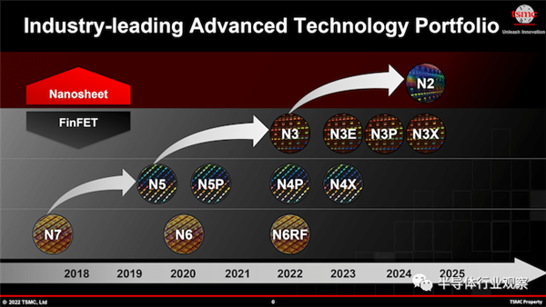
3nm, a new milestone for TSMC
According to TSMC, the company’s 3-nanometer (N3) process technology will be another full-generation process after the 5-nanometer (N5) process technology. When the N3 process technology is launched, it will be the most advanced process technology in the industry. Excellent PPA and transistor technology.
Compared with N5 process technology, the logic density of N3 process technology will increase by about 70%, and the speed will increase by 10-15% at the same power consumption, or the power consumption will be reduced by 25-30% at the same speed.
However, N3 has a relatively narrow process window (the range of parameters that yield defined results) and may not be suitable for all applications in terms of throughput. Also, as manufacturing processes become more complex, their wayfinding, research and development times get longer, so we no longer see TSMC and other foundries popping up a whole new node every two years.
For N3, TSMC’s new node introduction cycle will be extended to about 2.5 years. That means TSMC will need to offer an enhanced version of N3 to meet the needs of its customers who are still looking for performance-per-watt improvements and transistor density increases every year or so.
At the 2022 Tech Symposium, TSMC also discussed four N3-derived manufacturing processes (a total of five 3nm-class nodes)—N3E, N3P, N3S, and N3X—that will be launched in the next few years.
These N3 variants are designed to provide an improved process window, higher performance, higher transistor density and enhanced voltage for ultra-high performance applications.
Among them, N3E improves performance, reduces power consumption, and increases the process window, thereby improving brightness. But at the cost of slightly lower logic density at that node.
Compared with N5, N3E will reduce power consumption by 34% (at the same speed and complexity) or improve performance by 18% (at the same power and complexity), and increase logic transistor density by 1.6 times.
According to reports, TSMC will launch N3P (a performance-enhanced version of its manufacturing process) as well as N3S (a density-enhanced version of the node) sometime around 2024.
But TSMC has not revealed more information about these variants at this time. For those customers who require ultra-high performance regardless of power consumption and cost, TSMC will offer N3X, which is essentially the ideological successor of N4X. Again, TSMC didn’t reveal details about the node other than to say it will support high drive currents and voltages.
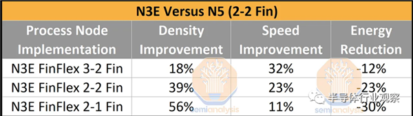
It’s worth mentioning that all of TSMC’s technologies will support FinFlex, a TSMC “secret sauce” feature that greatly increases design flexibility and allows chip designers to precisely optimize performance, power consumption, and cost. In short, FinFlex allows chip designers to precisely tailor their building blocks to achieve higher performance, higher density and lower power consumption.
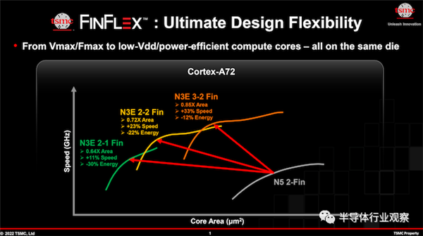
In practice, TSMC’s FinFlex technology will allow chip designers to mix and match different types of standard cells within a block to precisely tailor performance, power consumption and area. For complex structures like CPU cores, this optimization provides many opportunities to increase core performance while still optimizing die size.
However, we must emphasize that FinFlex is not a substitute for node specialization (performance, density, voltage) as process technologies have greater variance in libraries or transistor structures than within a single process technology, but FinFlex appears to be the best way to optimize performance, power And a good way to cost TSMC’s N3 node. Ultimately, this technology will bring the flexibility of FinFET-based nodes closer to that of nanosheet/GAAFET-based nodes, which will offer adjustable channel widths for higher performance or lower power consumption.
Samsung 3nm, got up early
In fact, long before TSMC announced 3nm mass production, Samsung had already announced that it had achieved mass production of 3nm process.
In June 2022, Samsung announced that it had started initial production of its 3 nanometer (nm) process node using a gate-all-around (GAA) transistor architecture.
The multi-bridge channel FET (MBCFET ) used in it is the first GAA technology adopted by Samsung. This process breaks through the performance limitation of FinFET, improves power efficiency by reducing the power supply voltage level, and improves performance by increasing the drive current capability.
The company is also beginning to use nanosheet transistors with semiconductor chips for high-performance, low-power computing applications, with plans to expand to mobile processors.
Samsung said that using nanosheets with wider channels with the company’s proprietary technology can achieve higher performance and higher energy efficiency than GAA technology using nanowires with narrower channels.
Using 3nm GAA technology, Samsung will be able to adjust the channel width of the nanosheets to optimize power consumption and performance to meet various customer needs.
In addition, the design flexibility of GAA is very conducive to design technology co-optimization (DTCO), which can help improve power, performance, area (PPA) advantage.
Compared with the 5nm process, the first-generation 3nm process can reduce power consumption by up to 45%, improve performance by 23%, and reduce area by 16%, while the second-generation 3nm process can reduce power consumption by up to 50% and improve performance by 30% %, the area is reduced by 35%.
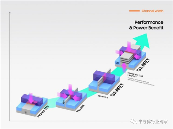
As mentioned above, unlike TSMC’s process, Samsung’s 3nm uses GAA transistors, which opens a new era.
Samsung has been working on 3nm/GAAFET technology since they originally announced the technology in 2019. Samsung’s unique GAA transistor technology is the Multi-Bridge Channel FET (MBCFET), which is a nanosheet-based implementation.
Nanosheet-based FETs are highly customizable, and the width of the nanosheets is a key metric defining power and performance characteristics: the larger the width, the better the performance (at higher powers). Thus, transistor designs focused on low power consumption can use smaller nanosheets, while logic requiring higher performance can use wider nanosheets.
In the early days of Samsung’s 3nm release, industry insiders have been criticizing its yield rate, but according to industry sources in January this year, Samsung Electronics on Monday sharply increased the yield rate of the industry’s most advanced 3nm chip produced for fabless customers. yield.
Samsung’s first-generation 3nm process node has achieved “perfect levels” of production yield, the person said, without elaborating further.
Previously, Taiwanese media reported that TSMC’s 3nm process production yield was as high as 85%, higher than Samsung. But South Korean industry sources played down the report, saying the figure appeared to be inflated.
They said that considering TSMC provides Apple with the mass production and delivery schedule of the industry’s smallest chip, its production yield rate is at most 50%.
According to the media, because of the failure of the first generation of 3nm, Samsung is investing heavily in the research and development of the second generation process.
The report disclosed that Samsung’s second-generation 3nm GAA process will be mass-produced in 2024, and the process will be added to the MBCFET architecture, and the performance will also be improved a lot.
While Samsung did not share statistical differences for the 4nm node, the second-generation 3nm GAA is still expected to reduce power consumption by as much as 50%, improve performance by 30%, and reduce die area by 35% compared to the company’s 5nm process.
The giants join forces at 2 nanometers, a decisive battle
Although both Samsung and TSMC have spent a lot of thought on 3nm, it can be seen from past news and manufacturers’ announcements that it seems that everyone is not interested in the first-generation 3nm process. For example, it was once rumored in the market that Apple would become the only customer of TSMC’s first-generation 3nm process. However, the US giant has not announced its 3nm products so far.
It can be seen that it is an industry consensus that the first generation of 3nm is not optimistic. But the market’s pursuit of craftsmanship has not stopped at present. In addition to these two foundries, Intel will also reportedly launch its 3nm process node by the end of 2023. And they seem to have set their sights on 2nm.
At that time, Intel’s Intel 20A (2nm) will usher in the Angstrom era, using GAA (RibbonFET) transistors and PowerVia technology to improve power retention.
Intel rival TSMC will adopt GAA at its 2nm node in 2025, giving chipmakers a head start as they hit the limits of miniaturization. Plus Japanese start-ups Rapidus and Samsung, which will have a 2nm prototype line in 2025.
For chip companies, how to face chip design challenges and cost challenges will be their top priority for many years to come.
[ad_2]
Source link